

Integrated circuits are mostly built on Silicon wafer material. Many different devices - like transistors, diodes or capacitors - are connected by multiple interconnect layers. Thin film and furnace processes are followed by masking steps which consist of a structuring lithography process and a subsequnet etch process. These sequencies require intensive metrology processes to keep the process in a certain window. MueTec offers a wide variety of metrology and measurement processes, like:
- Critical Dimension or CD Measurement like active area, gate length or contact diameter
- Modern manufacturing processes consist of 30 and more masking levels which have to be perfect in Overlay
- Film thickness measurement of transparent films like Oxide, Nitride or Photo resist
- Defects and their reduction play a important role in the overall profitability of a manufacturing line. Therefore Defect Inspection and Review are important tools for engineers to increase yield.
- Since Silicon is transparent to IR radiation - we are utilizing this optical band for Infrared Inspection & Measurement to look deep into the wafer structure without damaging it.
Get in Touch

Reasons to Choose MueTec
Since decades we are listening to your manufacturing challenges and, together with you, find solutions to solve them successfully. You are invited to benefit from our accumulated know how that translates into tools, software algorithms and application support.
The installed base of our tools reaches from volume semiconductor manufacturers to mask shops and research institutes. We installed and service hundreds of tools all around the world. The satisfaction of our customers drives our motivation to exceed their expectations.
We are proud to provide the flexibility to adopt our solutions to your individual requirements. All of us at MueTec understand that one size does not fit all and we are proud of our ability to adopt to your special needs in a fast and competent fashion.
Our existing customers value the robustness of our tools, many of them being in use for 15 years or longer. All of our tools are designed and manufactured in Germany with highest quality standards.
Our Mission
MueTec serves the semiconductor equipment industry as well as a number of other, closely related industries. Our systems, services and software algorithms help nanoelectronics manufacturers manage yield and minimize waste throughout their manufacturing process, from research and development to final mass production.
- Cost-effective solutions
- Your metrology and inspection specialist
- Installed base of more than 250 systems
- Local service and maintenance from certified technicians
Best Solutions for Si-Wafer
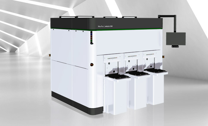
Argos 300
200mm/300mm Wafer Macro Defect InspectionShow details
Key Features
300 mm FOUP based handling
Data acquisition perfectly balanced to mechanical movements
Simultaneous bright- and darkfield front and backside inspection
Modular design with 1 – 3 process chambers, depending on throughput requirements
No recipe required for ease of use:
Enables productivity gains through minimum recipe customization
Ideal for fabs and packaging areas with many different devices & die sizes
No knowledge about geometry and physical parameters needed
Die layout data is not necessary
Recognition of active die area and EBR zone
Different sensitivities for different wafer areas
Avoiding false positives at zone transitions
Automatic adjustment of light intensity
Reflectivity of inspected layer is not necessary
Automatic defect recognition parameters by adaptive software algorithm
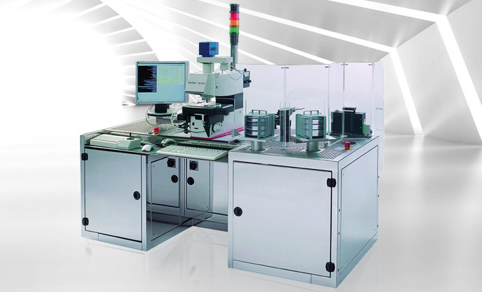
MT3000
Fully automated metrology and inspection system (open cassette)Show details
Typical Applications
CD
Overlay
Film Thickness
Defect Inspection
Defect Review
Features
VIS, UV
Simultaneous wafer handling 75 - 200mm
SECS/GEM
MT5500 / MT7500
Large area metrology and inspection system
Show details
Features
CD > 0,3 micron
contact holes > 0,3 micron
chrome and phase shift
resist on chrome
line edge roughness
substrate size up to 550mm x 550mm
DUV, 248nm; UV 365nm
DUV, UV, VIS
reflected and transmitted light
Substrates
large area scales
plastic electronics
glass scales
special customized solutions
Individual Inquiry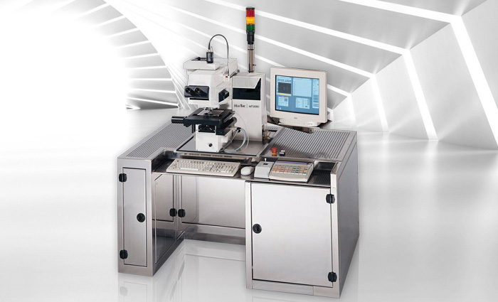
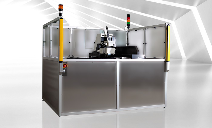
MT2010
Fully automated metrology and inspection system (open cassette)Show details
The MT2010 is designed for high precision defect inspection and metrology tasks on masks up to 6”. The system uses different illumination sources in transmitted and reflected light such as visible, I-line (365nm) and DUV (248nm).
MT2010 comes with laser autofocus and an anti-vibration isolating base frame with light tower.