

Micro-Electro-Mechanical-Systems - short: MEMS - can be defined as a technology which is using common Silicon processes to manufacture miniaturized mechanical and electro-mechanical devices. In contrast to the common IC processes in MEMS technology CD's vary from well below 1micron to few milimeters. Based on our IC manufacturing experience we are able to address the MEMS metrology requirements as well. Especially our Infrared Inspection & Measurement system addresses many aspects of MEMS metrology.
- Eutectic bonding and glass frit sealing inspection
- Device inspection of the MEMS structure
- CD and Overlay inspection
Get in Touch

Reasons to Choose Muetec
Since decades we are listening to your manufacturing challenges and, together with you, find solutions to solve them successfully. You are invited to benefit from our accumulated know how that translates into tools, software algorithms and application support.
The installed base of our tools reaches from volume semiconductor manufacturers to mask shops and research institutes. We installed and service hundreds of tools all around the world. The satisfaction of our customers drives our motivation to exceed their expectations.
We are proud to provide the flexibility to adopt our solutions to your individual requirements. All of us at MueTec understand that one size does not fit all and we are proud of our ability to adopt to your special needs in a fast and competent fashion.
Our existing customers value the robustness of our tools, many of them being in use for 15 years or longer. All of our tools are designed and manufactured in Germany with highest quality standards.
Our Mission
MueTec serves the semiconductor equipment industry as well as a number of other, closely related industries. Our systems, services and software algorithms help nanoelectronics manufacturers manage yield and minimize waste throughout their manufacturing process, from research and development to final mass production.
- Cost-effective solutions
- Your metrology and inspection specialist
- Installed base of more than 250 systems
- Local service and maintenance from certified technicians
Best Solutions for MEMS
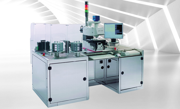
IRIS2100
200mm MEMS inspection and metrology system (open cassette)Show details
Typical Applications
MEMS Sealing Inspection
MEMS Device Inspection
Overlay/CD Metrology
Defect Review
Features
Best IR image quality
Flexible handling (backside vacuum, flipping, edge-vacuum) for MEMS specific wafers
Combined reflected & transmitted light illumination modes
SECS/GEM
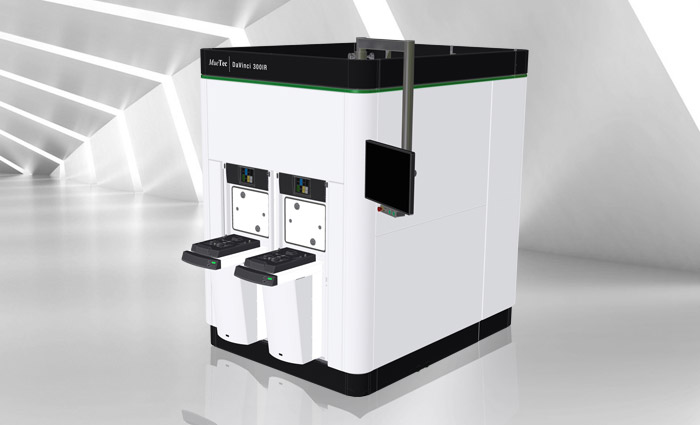
DaVinci 200IR + 300IR
200mm MEMS inspection and metrology system (SMIF)Show details
Typical Applications
Sealing Inspection after bonding
(eutectic bonding or glass frit bonding)
Device Inspection after bonding
Overlay Metrology after bonding
Critical Dimension Metrology after bonding
Features
Best inclassIR image quality with wafelengths of up to 1500nm
Flexible handling (backside vacuum, flipping, edge-vacuum) for MEMS specific wafers
Combined reflected & transmitted light illumination modes
SECS/GEM