

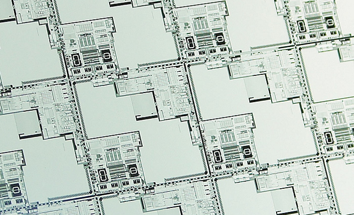
In modern Silicon based manufacturing technology there are numerous masking layers, each masking step requires its own mask. Each mask is using a glass substrate usually with a Cromium pattern. Obviously the mask must fulfill stringent requirements concerning the CD transfer to the wafer and in addition the defects have to be driven to the absolute possible minimum. Based on extensive know how in this area MueTec offers:
- Critical Dimension measurement are a typical application to improve manufacturing yield
- Film thickness measurement of transparent films like Oxide, Nitride or Photo resist
- Defect inspection and review play an important role in order to prevent masks from becoming a limiting factor for overall yield
Get in Touch

Reasons to Choose Muetec
Since decades we are listening to your manufacturing challenges and, together with you, find solutions to solve them successfully. You are invited to benefit from our accumulated know how that translates into tools, software algorithms and application support.
The installed base of our tools reaches from volume semiconductor manufacturers to mask shops and research institutes. We installed and service hundreds of tools all around the world. The satisfaction of our customers drives our motivation to exceed their expectations.
We are proud to provide the flexibility to adopt our solutions to your individual requirements. All of us at MueTec understand that one size does not fit all and we are proud of our ability to adopt to your special needs in a fast and competent fashion.
Our existing customers value the robustness of our tools, many of them being in use for 15 years or longer. All of our tools are designed and manufactured in Germany with highest quality standards.
Our Mission
MueTec serves the semiconductor equipment industry as well as a number of other, closely related industries. Our systems, services and software algorithms help nanoelectronics manufacturers manage yield and minimize waste throughout their manufacturing process, from research and development to final mass production.
- Cost-effective solutions
- Your metrology and inspection specialist
- Installed base of more than 250 systems
- Local service and maintenance from certified technicians
Best Solutions for Mask
Spector-A
Fully automated mask metrology and inspection systemShow details
Typical Applications
CD
Defect Inspection
Features
Mask sizes up to 8“ by 8“
Robot handling
SECS/GEM
VIS, UV
Also available as semi-automated system with manual mask loading (Spector-M)
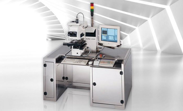
MT2010
Fully automated metrology and inspection system (open cassette)Show details
The MT2010 is designed for high precision defect inspection and metrology tasks on masks up to 6”. The system uses different illumination sources in transmitted and reflected light such as visible, I-line (365nm) and DUV (248nm).
MT2010 comes with laser autofocus and an anti-vibration isolating base frame with light tower.
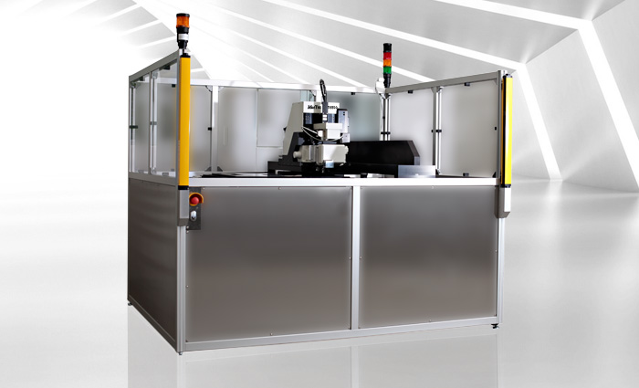
MT5500 / MT7500
Large area metrology and inspection system
Show details
Features
CD > 0,3 micron
contact holes > 0,3 micron
chrome and phase shift
resist on chrome
line edge roughness
substrate size up to 550mm x 550mm
DUV, 248nm; UV 365nm
DUV, UV, VIS
reflected and transmitted light
Substrates
large area scales
plastic electronics
glass scales
special customized solutions
Individual Inquiry