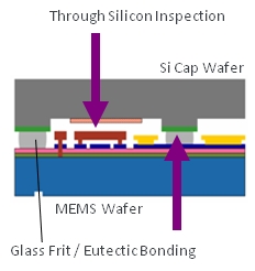
Silicon, GaAs wafers and other substrates become transparent at infrared (IR) wavelengths. High performance IR optics in combination with a high efficiency InGaAs camera provide images with superior resolution and contrast.
Advantages of MueTec solutions
- The optics are designed and optimized for the IR range from 1050 to 1550nm including IR optimized objective lenses with selectable magnifications from 2.5x, 5x, 10x, 20x, 63x, 100x.
- The high resolution InGaAs-camera guarantees best image resolution and highest contrast images.
- The IR optimized illumination path can be switched to incident and/or transmitted light.
- A combination of IR & visible light inspection is supported.
- The autofocus can be chosen between real-time laser autofocus or the highly intelligent fast image autofocus
- The best-in-class technology ensures worldwide leading edge performance regarding accuracy, repeatability and throughput.

CD & Overlay Measurement
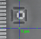
The combination of a high resolution objective lens (up to 100x) and our powerful NanoStar software solution guarantees the best available measurement accuracy with sub-micron repeatability for CD and overlay measurements. Our systems feature a unique combination of visible and infrared illumination in order to deliver optimized results for structures on the top, and the bottom, and inside the substrate.

Overlay top-to-bottom
Products

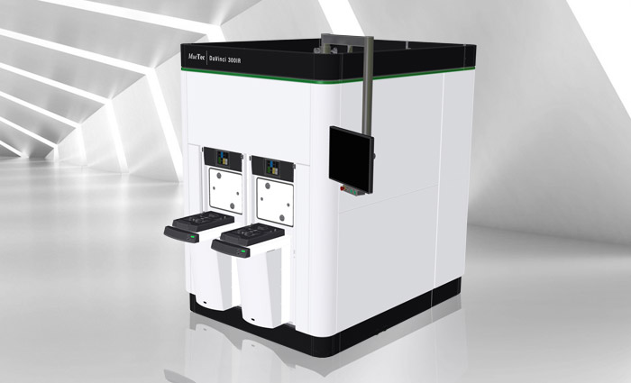
DaVinci 200IR + 300IR
200mm MEMS inspection and metrology system (SMIF)Show details
Typical Applications
Sealing Inspection after bonding
(eutectic bonding or glass frit bonding)
Device Inspection after bonding
Overlay Metrology after bonding
Critical Dimension Metrology after bonding
Features
Best inclassIR image quality with wafelengths of up to 1500nm
Flexible handling (backside vacuum, flipping, edge-vacuum) for MEMS specific wafers
Combined reflected & transmitted light illumination modes
SECS/GEM

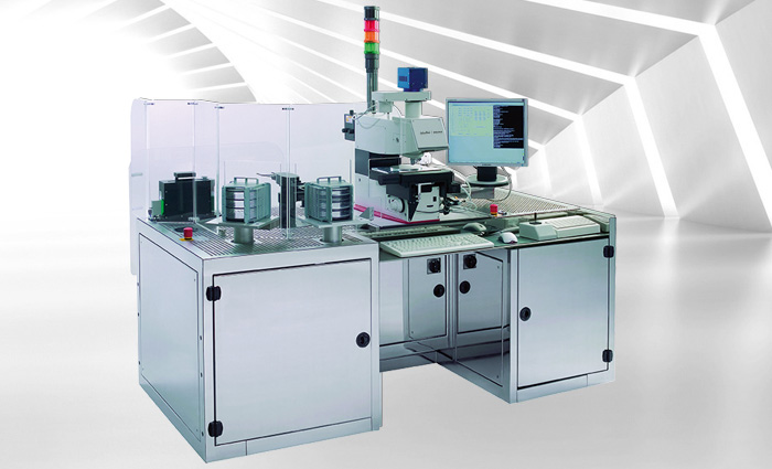
IRIS2100
200mm MEMS inspection and metrology system (open cassette)Show details
Typical Applications
MEMS Sealing Inspection
MEMS Device Inspection
Overlay/CD Metrology
Defect Review
Features
Best IR image quality
Flexible handling (backside vacuum, flipping, edge-vacuum) for MEMS specific wafers
Combined reflected & transmitted light illumination modes
SECS/GEM

