

High Throuput Macro Defect Inspection
MueTec’s Macro Defect Inspection products are designed for customers with many different wafer types. The system is easy to operate and does not require to write any recipes. It also enables 100% inspection of all wafer during the process of lithography with a throughput that is equal to, or faster that of a lithography cluster. In consequence, we enable our customers to move from sample inspection to inspection of all wafer and from manual inspection by operators to a statistically reliable, automated inspection process. Our tools can easily be setup without using much floor space. Low acquisition and operating costs guarantee a fast return on invest.
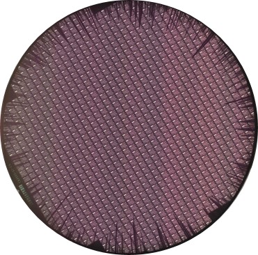
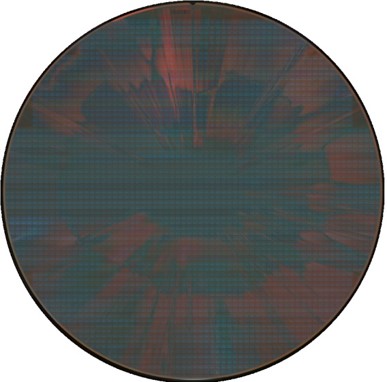
Here you can see an example of resist failure and an example resist streaks at lithography.
SIGNIFICANT ADVANTAGES
Enabling 100% wafer inspection at lithography
- Throughput 200 wafer per hour
- No recipe required for ease of use
- Replaces manual inspection
- Simulaneous wafer frontside and backside inspection
- Highly cost effective solution for fast return on inves
Products
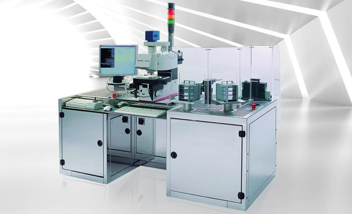
Rembrandt 200 / 300
200mm MEMS inspection and metrology system (SMIF)Show details
Typical Applications
Macro defect inspection of 200mm and 300mm wafer
Features
200mm SMIF or 300 mm FOUP based handling
Data acquisition perfectly balanced to mechanical movements
Illumination: Bright and darkfield, LED based
Black/white and colored image of sample
Modular system architecture results in small footprint
Design allows addition of 3rd module and 4th FOUP
Throughput optimized & balanced system integration avoids bottlenecks
MT3000
Fully automated metrology and inspection system (open cassette)Show details
Typical Applications
CD
Overlay
Film Thickness
Defect Inspection
Defect Review
Features
VIS, UV
Simultaneous wafer handling 75 - 200mm
SECS/GEM
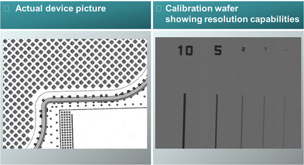
High Resolution Macro Defect Inspection
For customers with higher resolution requirements, MueTec provides a high resolution macro defect inspection solution down to 1μm.
SIGNIFICANT ADVANTAGES
- Recipe-less algorithm: Ideal for wafer fabs with many different product types
- Cost effective - replaces manual inspection
- Two simultaneous illumination modes (bright field, dark field)
- Throughput of 50 wph at 2µm/pixel resolution
- 300mm FOUP or 200mm SMIF version available
Products
Rembrandt 200 / 300
200mm MEMS inspection and metrology system (SMIF)Show details
Typical Applications
Macro defect inspection of 200mm and 300mm wafer
Features
200mm SMIF or 300 mm FOUP based handling
Data acquisition perfectly balanced to mechanical movements
Illumination: Bright and darkfield, LED based
Black/white and colored image of sample
Modular system architecture results in small footprint
Design allows addition of 3rd module and 4th FOUP
Throughput optimized & balanced system integration avoids bottlenecks