

MueTec’s Infrared-Solutions are designed to improve manufacturing yield in MEMS manufacturing. We offer fully automated solutions for 100 mm, 150 mm, 200 mm and 300 mm MEMS wafer. Our systems cover the following applications:
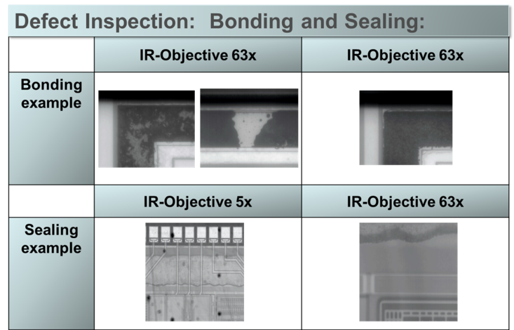
- Sealing Inspection after bonding (eutectic bonding or glass frit bonding)
- Device Inspection after bonding
- Overlay Metrology after bonding
- Critical Dimension Metrology after bonding
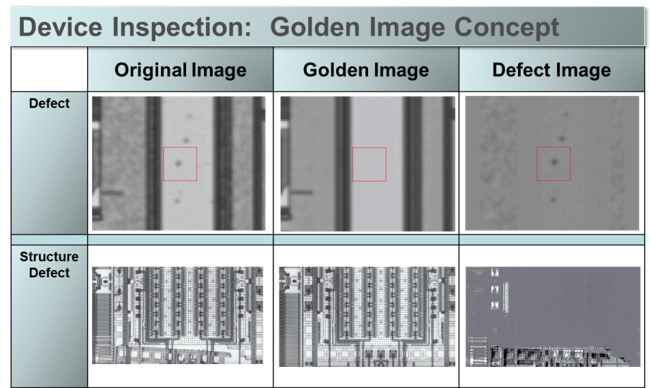
For device inspection, MueTec’s algorithms are working with a modified golden image concept. The algorithm features an automatic calculation of golden images during run-time. We refer to his method as “Smart Defect Inspection”, or SDI, as it greatly enhances throughput and usability. For large die sealing inspection, our sealing inspection module requires stitching of single images to one big image for final sealing defect analysis. Defects detected in the stitched images needs to be consolidated into one result for the entire die:
IRIS2100
200mm MEMS inspection and metrology system (open cassette)Show details
Typical Applications
MEMS Sealing Inspection
MEMS Device Inspection
Overlay/CD Metrology
Defect Review
Features
Best IR image quality
Flexible handling (backside vacuum, flipping, edge-vacuum) for MEMS specific wafers
Combined reflected & transmitted light illumination modes
SECS/GEM
DaVinci 200IR + 300IR
200mm MEMS inspection and metrology system (SMIF)Show details
Typical Applications
Sealing Inspection after bonding
(eutectic bonding or glass frit bonding)
Device Inspection after bonding
Overlay Metrology after bonding
Critical Dimension Metrology after bonding
Features
Best inclassIR image quality with wafelengths of up to 1500nm
Flexible handling (backside vacuum, flipping, edge-vacuum) for MEMS specific wafers
Combined reflected & transmitted light illumination modes
SECS/GEM