

MueTec has a long-standing experience in providing customized soft- and hardware solutions for in-situ defect identification on regular or irregular structures, employing advanced pattern recognition, object analysis, object modeling, and object filtering algorithms. On request, customized programming solutions allow for a cost-effective implementation of almost any substrate analysis.
Significant advantages
- MueTec tools are expandable for Defect Inspection purposes
- Mostly it is only a question of software extension
- Leading to reasonably Cost of Ownership
Automated defect inspection is usually based on the so called “golden image principle”: images of various substrates are compared to a pre-produced template image, ”the golden image” to identify defects for subsequent analysis and classification. MueTec offers a wide range of software tools exploiting this principle for semi-automated as well as fully automated defect inspection. Many industrial applications however do not allow for the “golden image” approach due to throughput constraints or, more often, due to the high variability in the substrate design and substrate processing.
The MueTec proprietary Smart Defect Inspection (SDI) algorithm is no longer dependent on wafer-to-wafer process variations because the “golden image” calculation for each wafer is performed as soon as enough dies have been analyzed.
What is defect scanning (or substrate scanning)?
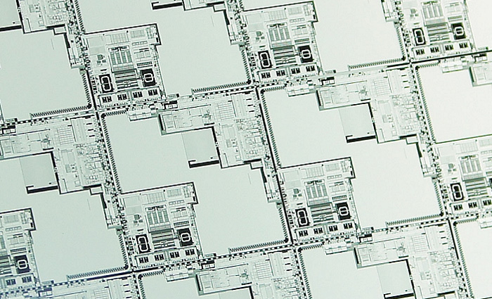
Defect scanning (or substrate scanning) describes an operation that completely images a selected area of a substrate or the complete substrate as a set of sub images. The scanning stage moves continuously either in the y- or x-direction and all CCD images are stored for defect evaluation. Stage speed and camera shot frequency are synchronized to guarantee that all areas of interest are covered. Cluster PCs process the images on-the-fly and handle a multitude of desired data evaluations. Freely adjustable filters defining e.g. defect size, defect area, defect morphology, location of the defect within the die or substrate ensure the flexibility of defect classification (defect type, defect severity) on any substrate.
MueTec supports die-to-die inspection with unlimited die size and even covers complete wafer comparison.
Products for Defect Inspection
Spector-A
Fully automated mask metrology and inspection systemShow details
Typical Applications
CD
Defect Inspection
Features
Mask sizes up to 8“ by 8“
Robot handling
SECS/GEM
VIS, UV
Also available as semi-automated system with manual mask loading (Spector-M)
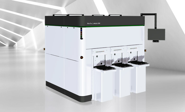
Argos 300
200mm/300mm Wafer Macro Defect InspectionShow details
Key Features
300 mm FOUP based handling
Data acquisition perfectly balanced to mechanical movements
Simultaneous bright- and darkfield front and backside inspection
Modular design with 1 – 3 process chambers, depending on throughput requirements
No recipe required for ease of use:
Enables productivity gains through minimum recipe customization
Ideal for fabs and packaging areas with many different devices & die sizes
No knowledge about geometry and physical parameters needed
Die layout data is not necessary
Recognition of active die area and EBR zone
Different sensitivities for different wafer areas
Avoiding false positives at zone transitions
Automatic adjustment of light intensity
Reflectivity of inspected layer is not necessary
Automatic defect recognition parameters by adaptive software algorithm
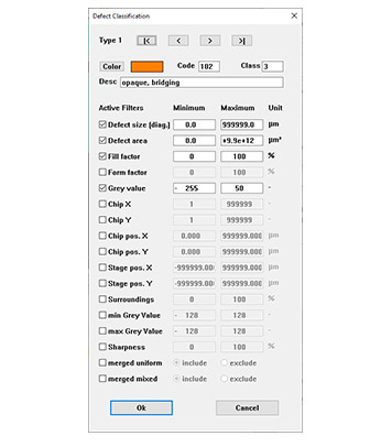 Example for freely definable filters for defect classification
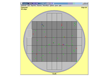 Result map of wafer inspection with classified
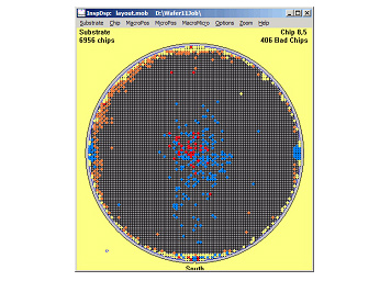 Result map of an infrared inspection of a sealed defects wafer …
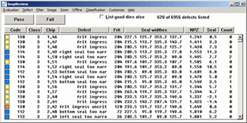 ...and the corresponding defect list