

Since decades we are listening to your manufacturing challenges and, together with you, find solutions to solve them successfully. You are invited to benefit from our accumulated know how that translates into tools, software algorithms and application support.
The installed base of our tools reaches from volume semiconductor manufacturers to mask shops and research institutes. We installed and service hundreds of tools all around the world. The satisfaction of our customers drives our motivation to exceed their expectations.
We are proud to provide the flexibility to adopt our solutions to your individual requirements. All of us at MueTec understand that one size does not fit all and we are proud of our ability to adopt to your special needs in a fast and competent fashion.
Our existing customers value the robustness of our tools, many of them being in use for 15 years or longer. All of our tools are designed and manufactured in Germany with highest quality standards.

Welcome to MueTec
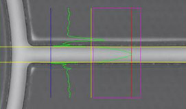
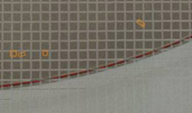
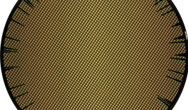
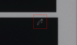
MueTec serves the semiconductor equipment industry as well as a number of other, closely related industries. Our systems, services and software algorithms help nanoelectronics manufacturers manage yield and minimize waste throughout their manufacturing process, from research and development to final mass production.
- Cost-effective solutions
- Your metrology and inspection specialist
- Installed base of more than 300 systems
- Local service and maintenance from certified technicians