

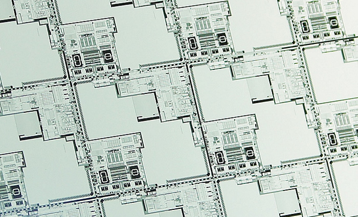
MueTec provides a comprehensive range of automated optical inspection (AOI) systems for various applications in the wafer and photomask industry, including CD (Critical Dimension) and Overlay Metrology, Defect Inspection, Defect Review and Film Thickness Measurement. These defect inspection and metrology equipment solutions are designed to support fabs expedite their development and production ramp cycles, to achieve higher semiconductor die yields and to improve return on invest.
Our products are also used in related industries, including wafer manufacturing, photomask manufacturing, MEMS and LED manufacturing and general materials research. Our portfolio ranges from stand-alone microscopes and semi-automated systems all the way to fully-automated products and systems. We support wafer sizes from 50.8 mm to 300 mm and mask sizes up to 750 mm. We invite you to visit sections of our website specific to your company’s metrology and inspection needs.
Products for Metrology & Inspection
Spector-A
Fully automated mask metrology and inspection systemShow details
Typical Applications
CD
Defect Inspection
Features
Mask sizes up to 8“ by 8“
Robot handling
SECS/GEM
VIS, UV
Also available as semi-automated system with manual mask loading (Spector-M)
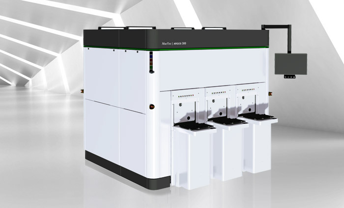
Argos 300
200mm/300mm Wafer Macro Defect InspectionShow details
Key Features
300 mm FOUP based handling
Data acquisition perfectly balanced to mechanical movements
Simultaneous bright- and darkfield front and backside inspection
Modular design with 1 – 3 process chambers, depending on throughput requirements
No recipe required for ease of use:
Enables productivity gains through minimum recipe customization
Ideal for fabs and packaging areas with many different devices & die sizes
No knowledge about geometry and physical parameters needed
Die layout data is not necessary
Recognition of active die area and EBR zone
Different sensitivities for different wafer areas
Avoiding false positives at zone transitions
Automatic adjustment of light intensity
Reflectivity of inspected layer is not necessary
Automatic defect recognition parameters by adaptive software algorithm
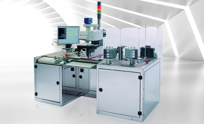
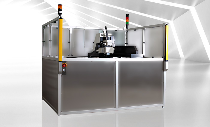
MT3000
Fully automated metrology and inspection system (open cassette)Show details
Typical Applications
CD
Overlay
Film Thickness
Defect Inspection
Defect Review
Features
VIS, UV
Simultaneous wafer handling 75 - 200mm
SECS/GEM
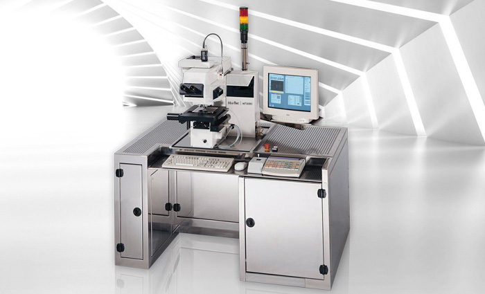
MT2010
Fully automated metrology and inspection system (open cassette)Show details
The MT2010 is designed for high precision defect inspection and metrology tasks on masks up to 6”. The system uses different illumination sources in transmitted and reflected light such as visible, I-line (365nm) and DUV (248nm).
MT2010 comes with laser autofocus and an anti-vibration isolating base frame with light tower.
MT5500 / MT7500
Large area metrology and inspection system
Show details
Features
CD > 0,3 micron
contact holes > 0,3 micron
chrome and phase shift
resist on chrome
line edge roughness
substrate size up to 550mm x 550mm
DUV, 248nm; UV 365nm
DUV, UV, VIS
reflected and transmitted light
Substrates
large area scales
plastic electronics
glass scales
special customized solutions
Individual Inquiry